Apparatus
The total surface area of CPTFT is 1,389 m2. CPTFT contains 15 individual experimental sections, including Advanced physical Vapor Deposition Lab Ⅰ, Advanced Chemical Vapor Deposition Lab, Advanced physical Vapor Deposition Lab Ⅱ, Thin Films & Mechanical Properties Testing Lab, Advanced Plasma Lab, Optoelectronic Measurement Lab, Industry-Processing Lab, Industry-testing Equipment Lab, Applied Biological Thin Films Lab, Liquid Plasma Lab, Plasma Surface Engineering Lab, Functional Atmospheric Plasma Lab, Plasma & Vacuum Technology Training Lab, Corrosion Prevention & Control Lab, Thin Film And Material Simulation Lab, as well as an office room and a multi-functional meeting room.
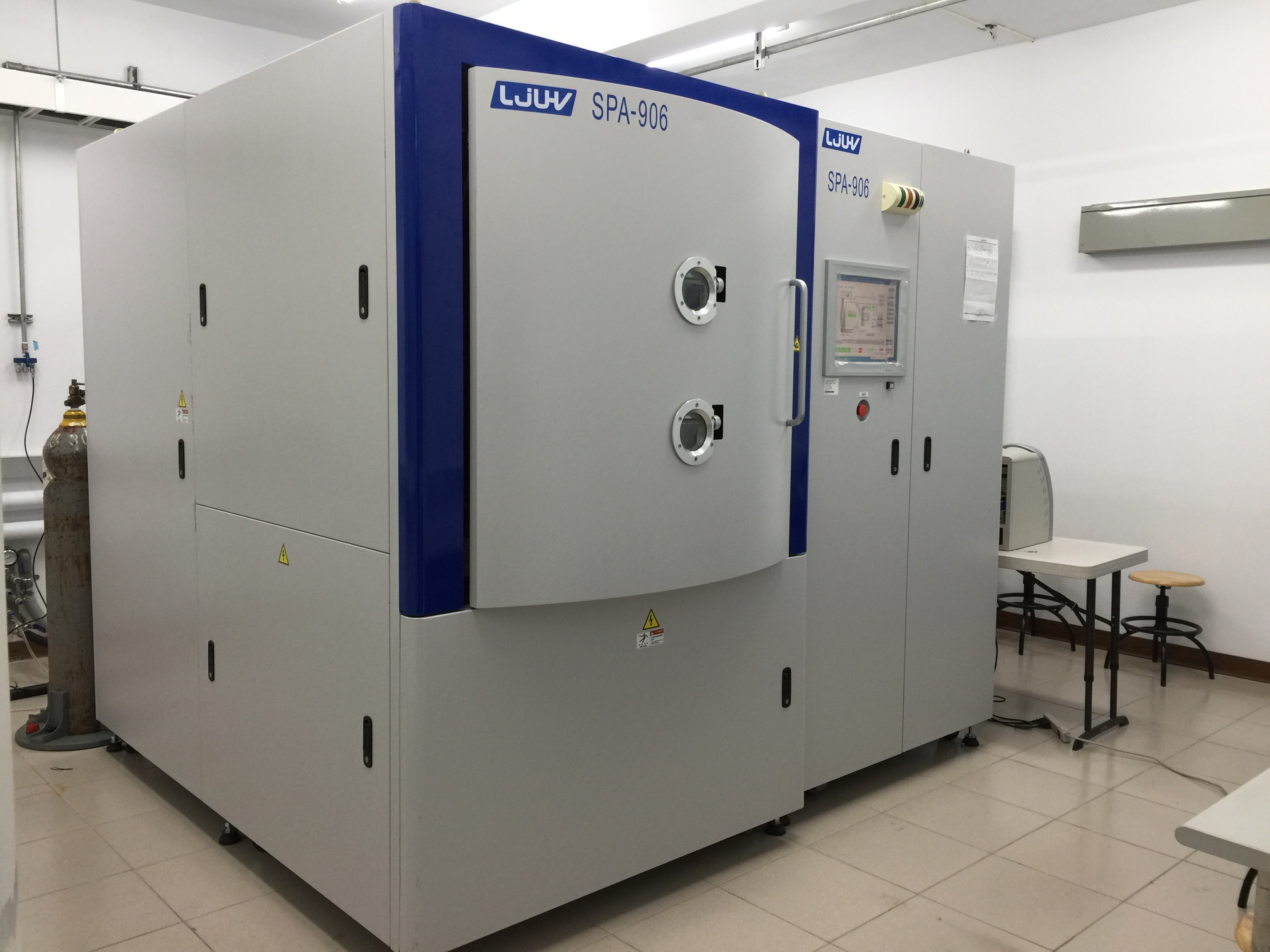
Advanced Chemical Vapor Deposition Lab.
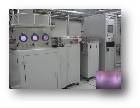
Inductively Coupled Plasma-Chemical Vapor Deposition, ICP-CVD
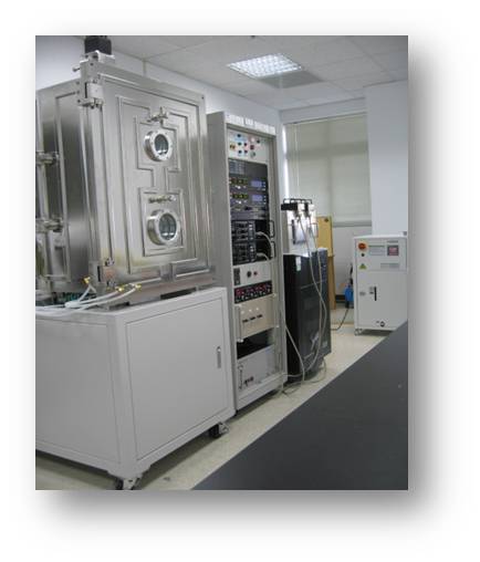
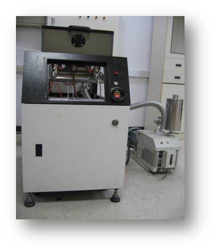
Advanced Physical Vapor Deposition Lab.Ⅰ
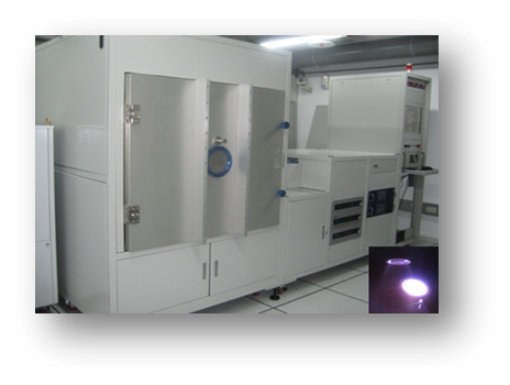
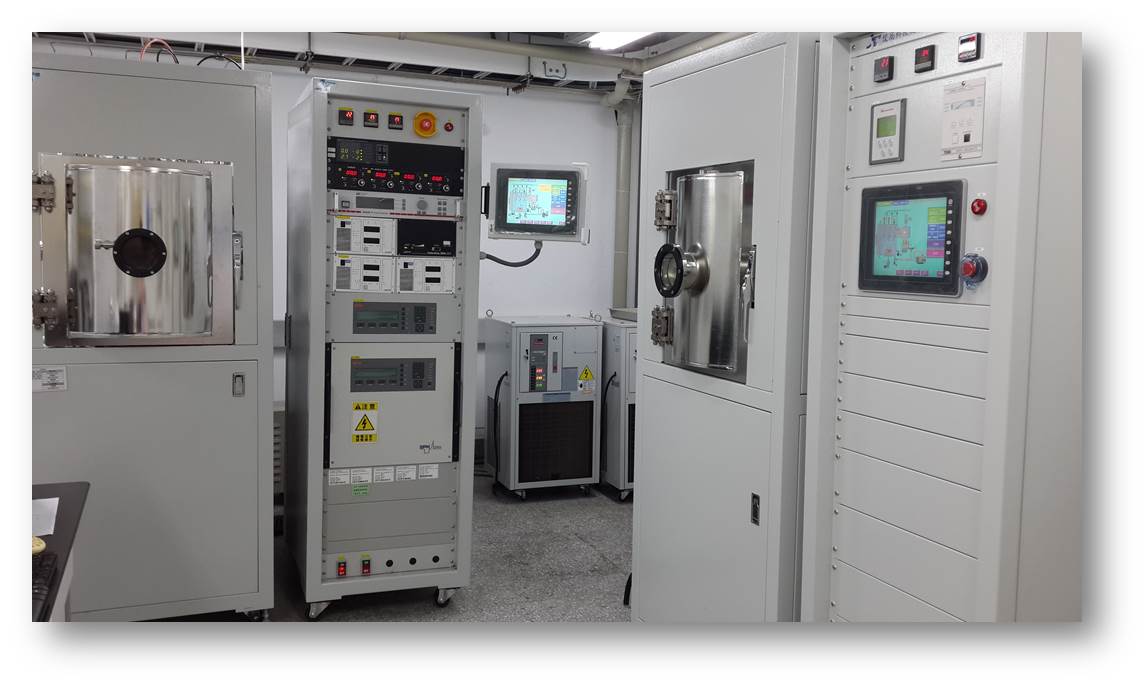
In- Line Physical Vapor Deposition
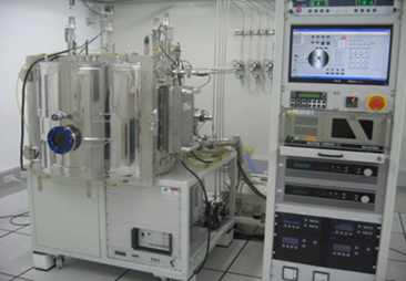
Batch Type Physical Vapor Deposition
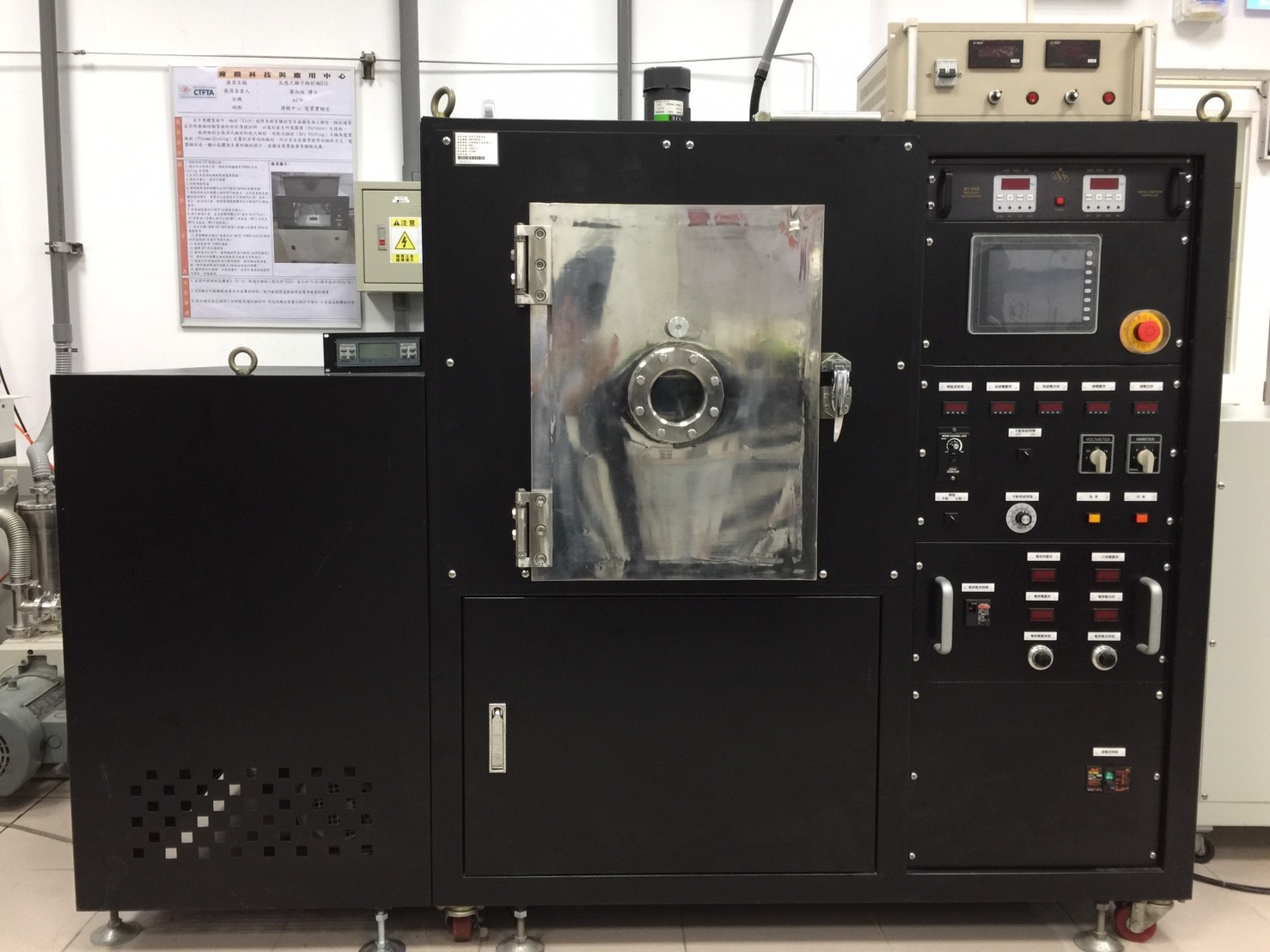
Advanced Physical Vapor Deposition Lab.Ⅱ
High Power Impulse Magnetron Sputtering, HIPIMS
Thin Films & Mechanical Properties Testing Lab.
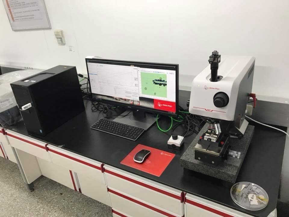
Scratch Tester
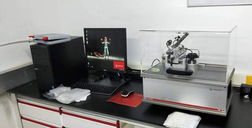
Tribometer
Thin Film Impact Tester
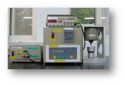
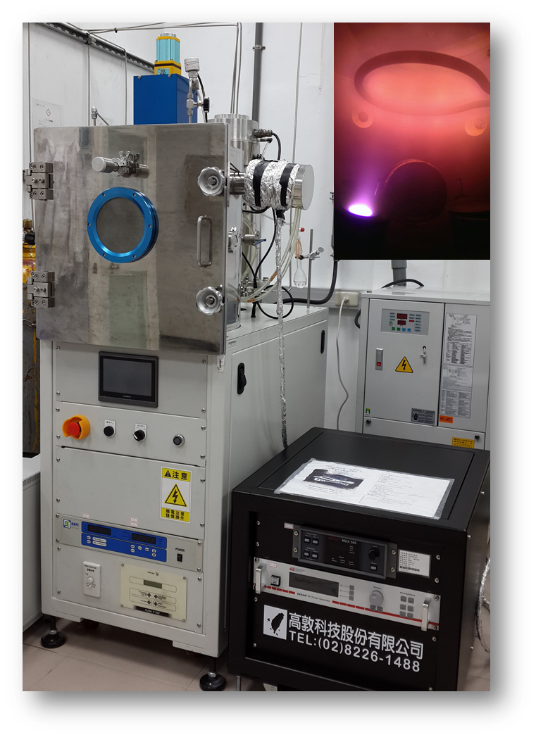
Advanced Plasma Lab.
Plasma Polymerization System
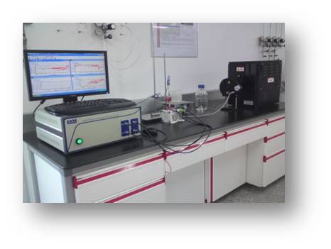
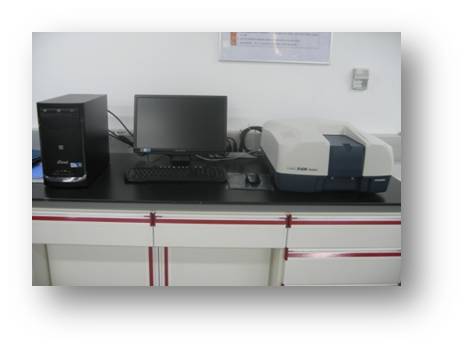
Optoeletronic Measurement Lab.
Photoelectrochemical Measuring System
UV-Visible Spectrophotometer)
Industry Process Lab.
Ion-Beam Assisted Deposition, IBAD
Reactive Ion Etcher, RIE
Deposition System
Organic-inorganic hybrid coating system
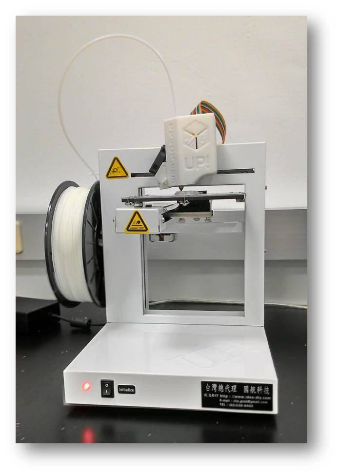
Industry-Testing Equipment Lab.
3D print
Electro-spinning
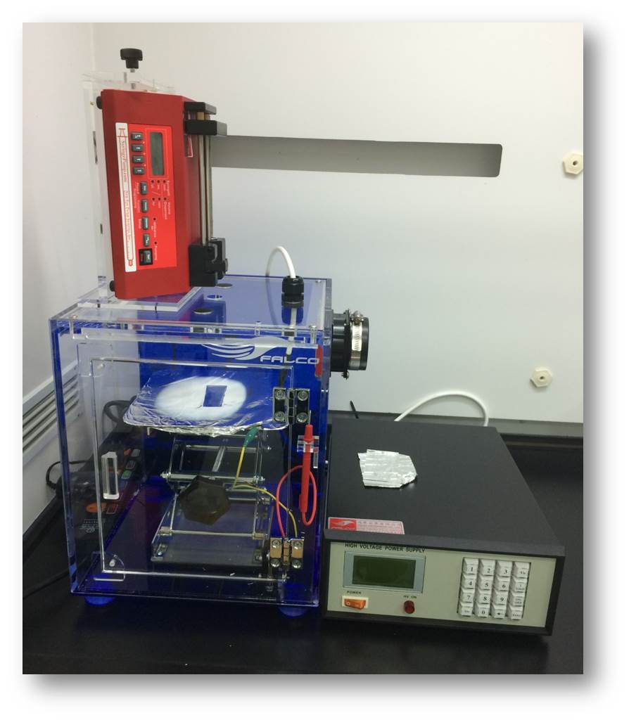
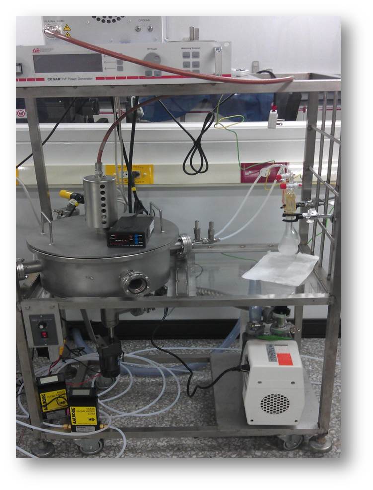
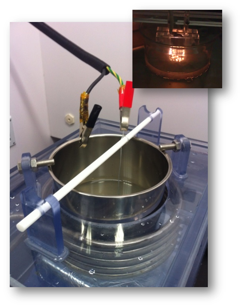
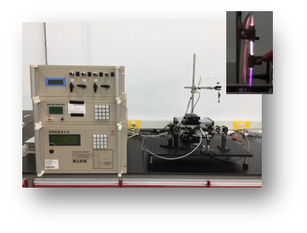
Solution Plasma Lab.
Solution Plasma System
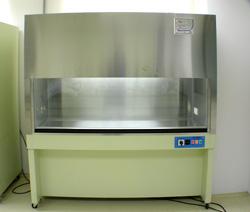
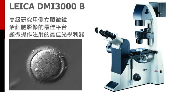
Applied Biological Thin Films Lab.
Laminar Flow
Microscope
Plasma Surface Engineering Lab.
Functional Atmospheric Plasma Lab.
Bio-Plasma System
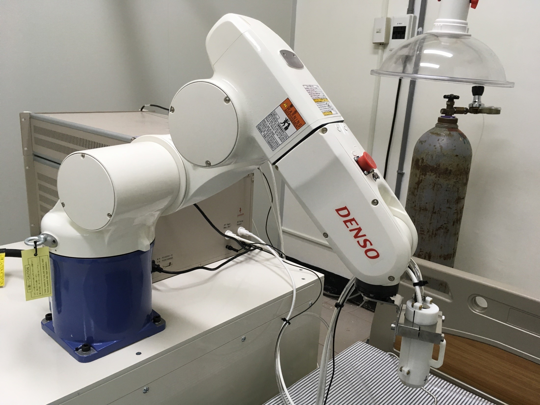
機械手臂